As electronics continue to advance at a rapid pace, the demand for more efficient and high-performing transistors has never been greater. Silicon-based transistors, although widely used, come with inherent limitations that hinder their performance. This has led electronics engineers and materials scientists to explore alternative materials that could potentially revolutionize the field of electronics.
One promising candidate that has captured the attention of researchers is two-dimensional (2D) semiconductors. These materials offer unique properties that could address the shortcomings of traditional silicon-based transistors. One of the key advantages of 2D semiconductors is their atomically thin nature, coupled with high carrier mobilities. These qualities make them ideal for enhancing the electrostatic control and ON-state performances of field-effect transistors (FETs) with short channels.
Despite the many advantages of 2D semiconductors, they are not without their challenges. One major limitation is the high contact resistances associated with Fermi-level-pinning effects. These effects significantly impact the performance of 2D transistors, making large-scale fabrication difficult. However, a recent study by researchers at Peking University and Chinese Academy of Sciences has introduced a novel yttrium-doping strategy to address this key limitation.
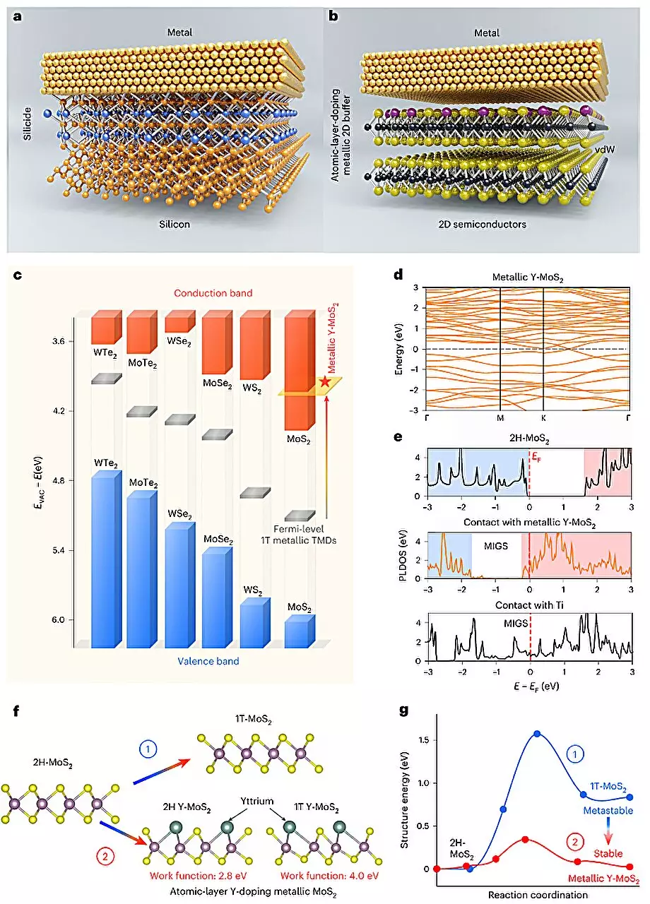
The yttrium-doping strategy involves converting semiconducting molybdenum disulfide (MoS2) into a metallic form, thereby improving band alignment and enabling the fabrication of ohmic contacts for 2D transistors. By introducing a semi-metal layer between a metal electrode and the 2D semiconductor, the efficiency of carrier injection is enhanced, reminiscent of traditional silicide structures in silicon-based transistors.
The researchers developed a plasma-deposition-annealing (PDA) method for yttrium doping in the surface layer of MoS2. This process involved treating patterned local contact areas with low-power soft plasma to create active sites, followed by the deposition of a Y/Ti/Au stacked metal with a 1 nm-thick active metal Y as a solid-state doping source. The Y atoms diffused into the active sites and were activated through high-temperature annealing in an inert gas environment.
The introduction of yttrium doping induced a 2D phase transition in MoS2, leading to metallization and overcoming traditional engineering limitations related to doping depth. The researchers were able to achieve a doping depth as thin as 0.5 nanometers, paving the way for ultra-short MoS2-based channel ballistic transistors with excellent performance as ohmic contacts and switching capabilities.
Future Implications
Looking ahead, the development of p-type ohmic contacts for 2D semiconductors could further enhance the potential of these materials in advanced electronics. The breakthrough yttrium-doping strategy opens up possibilities for creating sub-1 nanometer node chips with exceptional performances and low power consumption, setting the stage for the next generation of electronic devices. The research conducted by Chenguang Qiu and his colleagues marks a significant step towards unlocking the full potential of 2D semiconductors in the realm of electronics.


Leave a Reply