Two-dimensional (2D) semiconducting materials have sparked interest in the field of electronics due to their unique optoelectronic properties. These materials hold the potential for the development of ultra-thin and tunable electronic components. Despite this promise, integrating 2D semiconductors with gate dielectrics has presented challenges in the past, resulting in interfacial traps that limit transistor performance.
Researchers at King Abdullah University of Science and Technology (KAUST), Soochow University, and collaborating institutes introduced a novel approach to address these challenges. Their innovative design involved the use of hexagonal boron nitride (h-BN) dielectrics and metal gate electrodes with high cohesive energy. By utilizing platinum (Pt) as an anode, the researchers observed a significant reduction in dielectric breakdown when compared to traditional gold (Au) electrodes. This led to a 500-times lower leakage current and a dielectric strength of at least 25 MV/cm in Pt/h-BN gate stacks.
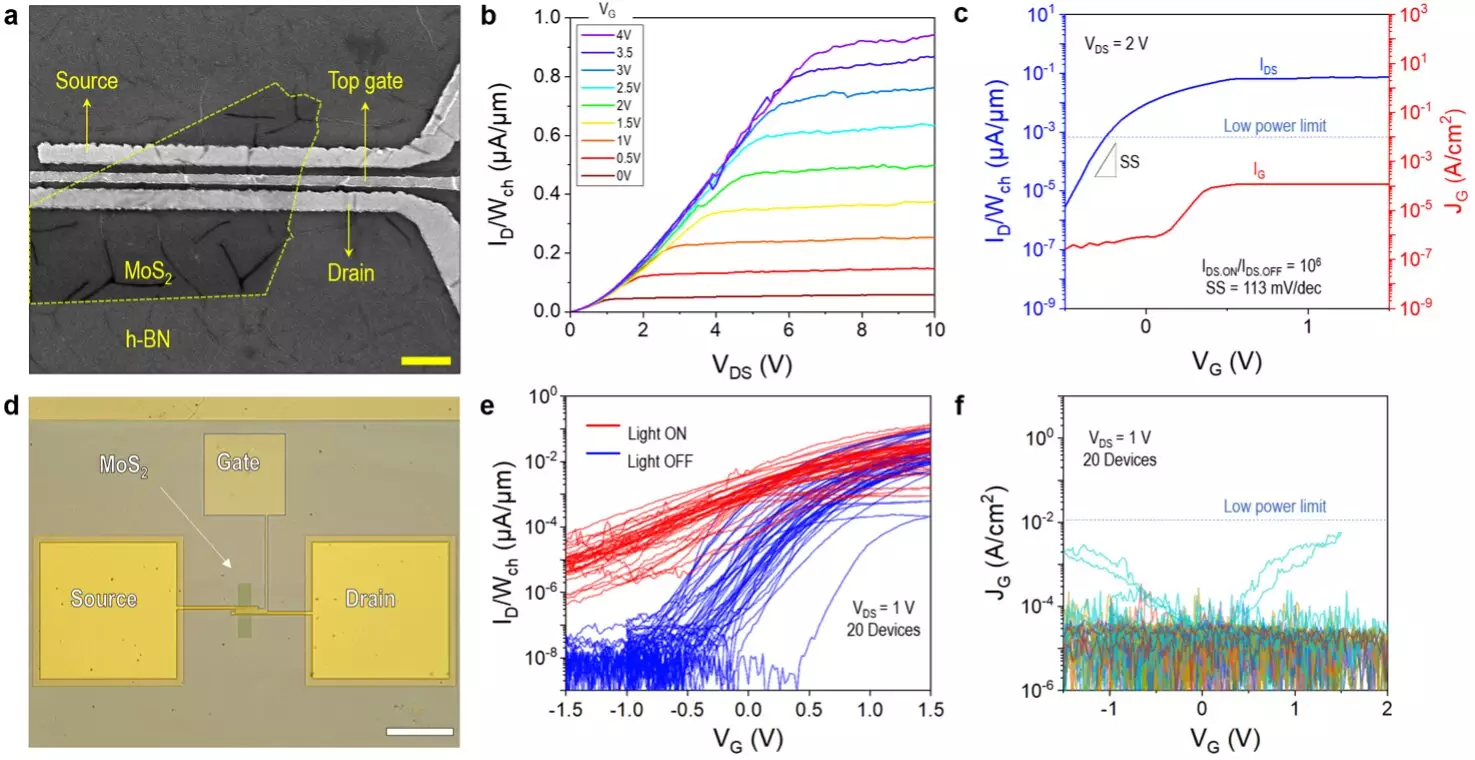
Yaqing Shen, the first author of the study, along with Prof. Mario Lanza and their colleagues, conducted experiments using chemical vapor deposited h-BN as dielectrics. They fabricated over 1,000 devices to evaluate the performance of h-BN gate dielectrics in conjunction with high cohesive energy metals such as Pt and tungsten (W). Utilizing a vertical Pt/h-BN/MoS2 structure, the researchers meticulously cleaned the substrate, patterned the source and drain electrodes, deposited the MoS2 channel, and transferred the CVD h-BN film to create a robust transistor platform.
The researchers discovered that the clean van der Waals interface between MoS2 and h-BN played a crucial role in enhancing the reliability and performance of the transistors. Contrary to previous beliefs, CVD h-BN proved to be an effective gate dielectric when paired with high cohesive energy metals like Pt and W. This synergistic combination reduced leakage currents and improved gate control, paving the way for more efficient 2D transistor devices.
The research team’s innovative approach has demonstrated promising results in reducing leakage currents and enhancing dielectric strength in 2D semiconductor-based transistors. By enabling the fabrication of reliable solid-state microelectronic circuits, this work opens up new possibilities for utilizing 2D materials in advanced electronic devices. The success of this study may inspire other research groups to explore similar approaches and materials, potentially leading to the development of highly performing 2D semiconductor-based devices. As the field advances, the researchers plan to further develop ultra-small, fully 2D transistors to contribute to the progression of Moore’s Law in semiconductor technology.
The integration of 2D semiconductor materials with optimized gate dielectrics and metal electrodes represents a significant advancement in the field of electronics. The unique properties of 2D materials combined with innovative fabrication techniques have the potential to revolutionize the performance and reliability of future electronic devices. As researchers continue to explore the possibilities offered by 2D semiconductors, the development of next-generation electronic components becomes increasingly feasible.


Leave a Reply