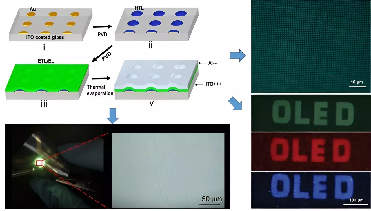
Organic semiconductors have become increasingly popular in various applications, ranging from OLED displays to biosensors. The use of these materials dates back to the 1980s when thin-film devices were first introduced. More recently, the demand for wearable electronics has pushed the development of organic semiconductors to achieve higher resolutions, especially in near-eye displays for virtual and augmented reality devices.
Researchers from Germany and China have been working on developing a photolithography-compatible technology for ultra-high-resolution organic semiconductor devices. The main challenge lies in the fact that traditional photolithographic methods, commonly used for inorganic semiconductors like silicon, do not work well with organic materials due to UV light and solvent damage. This limitation has led to alternative patterning methods with significantly lower resolutions, hindering the potential number of devices that can be integrated into a small area.
To overcome the limitations of traditional photolithography, researchers introduced a new strategy called “first surface patterning and then patterned growth.” This involves patterning the substrate surface with lithography before depositing organic semiconductor molecules. The molecules are then allowed to diffuse and selectively grow at designated areas, resulting in the formation of patterns and device fabrication on substrates. This innovative approach has enabled the creation of OLEDs with resolutions exceeding 20K ppi, meeting the demands for next-generation displays.
According to Lifeng Chi, the lead investigator of the study and a professor at Soochow University, this novel approach avoids the damage typically caused by lithographic procedures to organic semiconductors. The method offers significant advantages in terms of surface engineering and device resolution. Moving forward, it is believed that future wearable electronics will require the monolithic integration of multifunctional systems on a chip, encompassing information collection, transmission, processing, storage, and display.
The evolution of organic semiconductors in wearable electronics represents a significant advancement in the field of technology. With the development of innovative patterning methods and a focus on achieving ultra-high resolutions, organic semiconductor devices are poised to revolutionize the way we interact with electronic devices in the future.


Leave a Reply