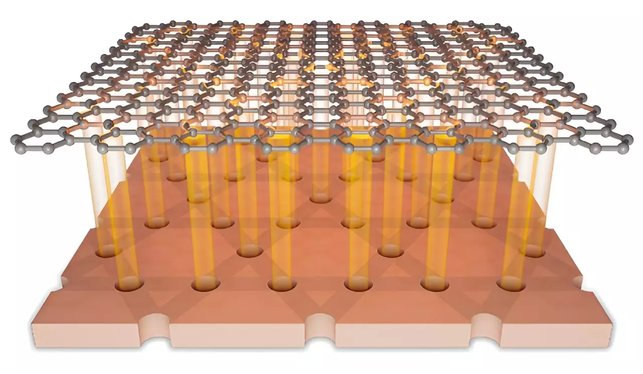
Advancements in materials science often hinge on the manipulation of electronic properties to foster innovations in technology. Among the most promising materials for such endeavors is graphene, a one-atom-thick layer of carbon known for its exceptional electrical, thermal, and mechanical properties. Recent research published in Physical Review Letters has introduced a groundbreaking method for selectively tuning electronic bands in graphene, marking a significant milestone in band structure engineering. Traditional techniques, while effective to a certain extent, fall short in offering real-time and continuous control over band structures, presenting an undeniable limitation for researchers and engineers aiming to harness the full potential of graphene.
Historically, methods such as heterostructuring, interfacial strain applications, and alloying have been employed for engineering electronic properties in materials. However, these conventional approaches have proven inadequate in providing the desired flexibility and scalability. They often lack the necessary precision required to tailor electronic bands to specific requirements actively. As research delves deeper into the worlds of van der Waals (vdW) materials and moiré heterostructures, the challenges surrounding band structure manipulation continue to provoke interest. The need for enhanced methodologies for controlling electronic properties and achieving bespoke material functionalities is evident, emphasizing the importance of continued research in this area.
Introducing the Kagome Superlattice: A Paradigm Shift
To address these challenges, the research team led by Prof. Zeng Changgan has proposed a novel method involving an artificial kagome superlattice to manipulate the Dirac bands in graphene. The key innovation of this study lies in the conception of a superlattice with a period of 80 nm—an essential factor enabling the folding and compression of high-energy bands to lower-energy regions. This significant transformation is instrumental for experimental observation and manipulation, presenting a host of new opportunities for researchers to explore.
The design of the kagome superlattice incorporates a high-order potential which facilitates intricate changes in band structures through various contributions. This characteristic allows for a nuanced approach to band modulation that is both selective and dynamic. By employing standard van der Waals assembly techniques in conjunction with electron beam lithography, the researchers achieved a functional kagome-lattice pattern that acts as a local gate for controlling graphene’s electronic response.
One of the most compelling aspects of this research is the ability to independently vary voltages across different components of the system. By altering the voltage applied to the local gate and the doped silicon substrate, the team managed to finely tune both the artificial potential strength and the carrier density in graphene. Such flexibility signifies a substantial leap forward in the ability to customize electronic properties on demand.
The researchers demonstrated that their high-order kagome potential not only allowed them to observe but also to manipulate the redistribution of spectral weight among various Dirac peaks—effectively showcasing a new layer of control over graphene’s electronic structure. Moreover, when a magnetic field was introduced, the impact of the superlattice on the band structure weakened, sustainably reactivating the intrinsic Dirac band. This dual control mechanism opens the door to even more sophisticated manipulation of electronic properties, expanding the toolbox available to materials scientists.
The implications of this research extend beyond mere academic curiosity. The method of employing artificial kagome superlattices for band engineering in graphene could usher in new technologies and applications, potentially sparking innovations across electronics, photonics, and energy sectors. This ability to finely control band structures heralds exciting possibilities for discovering novel physical phenomena and materials with functionalities tailored to meet specific needs.
The study led by the collaboration of eminent scientists from USTC, Wuhan University, and IMDEA Nanociencia marks a remarkable advancement in the ongoing quest to manipulate electronic properties of materials, particularly graphene. As research continues to develop and refine these techniques, the landscape of materials engineering stands on the verge of a revolutionary transformation, one that promises enhanced performance and novel applications in various fields.


Leave a Reply