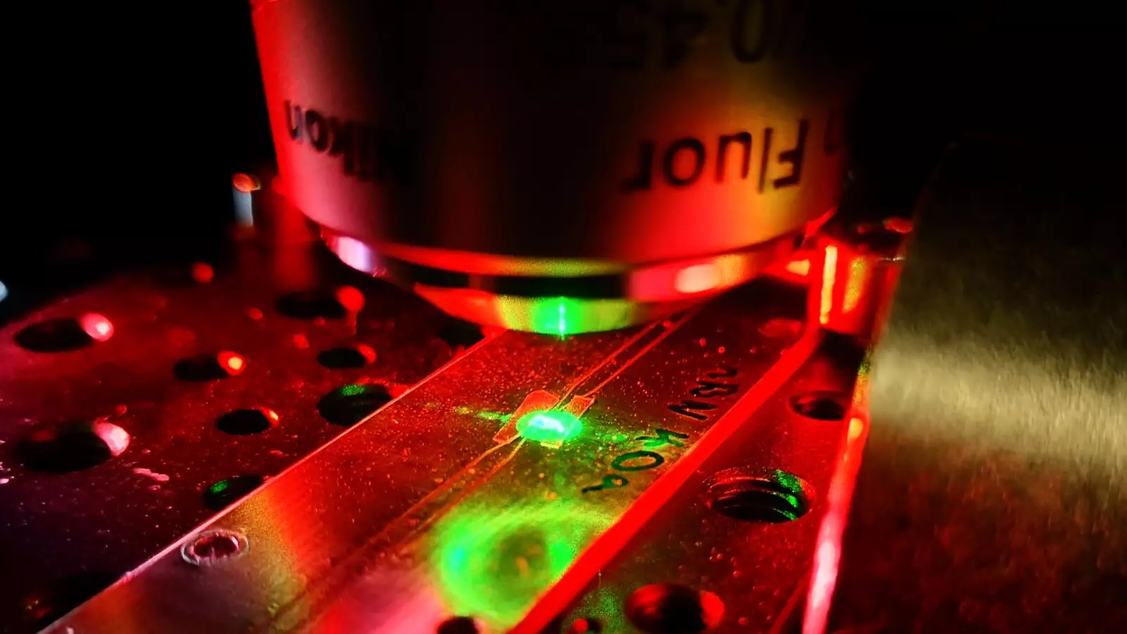
Quantum technology is advancing rapidly, with researchers at TMOS and RMIT University making significant strides in the field of quantum sensing. In a recent publication in Nature Communications, a new 2D quantum sensing chip using hexagonal boron nitride (hBN) was introduced. This groundbreaking thin-film format chip can detect temperature anomalies and magnetic fields in any direction simultaneously, leading to more versatile and cost-effective quantum sensors in the future.
Limitations of Diamond-Based Sensors
Traditionally, quantum sensing chips have been made from diamond due to its robust nature. However, diamond-based sensors have limitations, such as only being able to detect magnetic fields when aligned in a specific direction. This requirement for alignment results in large blind spots and the need for multiple sensors at varying degrees of alignment, making operation more complex and limiting versatility. Additionally, the rigid and three-dimensional nature of diamond sensors restricts their ability to get close to samples that are not perfectly smooth.
To address these challenges, researchers are turning to hexagonal boron nitride (hBN) as a new quantum sensing platform. HBN crystals are made up of atomically thin layers, making them flexible and allowing sensing chips to conform to the shape of the sample being studied. This flexibility enables the sensors to get much closer to the sample than diamond-based sensors can, opening up new possibilities for research and applications.
In their exploration of hBN, researchers discovered a new carbon-based defect with unique optical properties that allow it to detect magnetic fields in any direction. This defect behaves as a spin half system, enabling the sensor to detect magnetic fields with unprecedented versatility. The team also found that this defect could be controlled through electrical excitation, similar to the well-understood boron vacancy defect in hBN, and that they could be tuned to interact with each other.
The development of this new quantum sensing chip opens up a world of possibilities for applications in various fields. The isotropic sensor allows for the measurement of temperature and magnetic fields simultaneously, offering a versatile tool for research and industry. Potential applications include in-field identification of magnetic geological features and radio spectroscopy across a wider band than current technologies can provide.
The development of a 2D quantum sensing chip using hBN represents a significant advancement in the field of quantum technology. The unique properties of hBN, combined with the discovery of a new carbon-based defect, offer exciting prospects for the future of quantum sensing. Continued research and development in this area will pave the way for even more innovative applications and breakthroughs in the field of quantum materials and sensing devices.


Leave a Reply