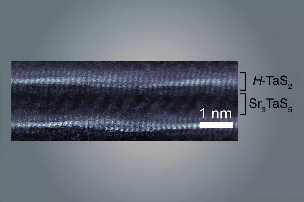
In a striking development from MIT, a team of physicists has unveiled a new class of materials characterized by their fascinating superconducting and metallic properties. This is achieved through the design of atomically thin, wavy layers, each measuring a mere billionth of a meter, that interlace to form a larger sample. The creation of such macroscopic samples opens avenues for detailed exploration of quantum behaviors, broadening our understanding of the atomic interactions responsible for unique material characteristics. The implications of this work, published in the prestigious journal *Nature*, extend beyond mere academic interest, potentially ushering in a new age in materials engineering where custom-designed substances can exhibit unusual and beneficial properties.
One of the most notable aspects of this research is its foundation in rational design—an approach that leverages scientific insights to engineer materials predictively. Traditionally, the synthesis of advanced materials can be erratic and unpredictable; however, this team applied a systematic methodology to produce their wavy structure, confident in their ability to iterate on their formula to devise further materials with intriguing effects. Their innovative synthesis employs a simple mix of powdered components, followed by exposure to elevated temperatures, prompting natural chemical reactions that yield large, manipulatable crystals. This significant breakthrough represents a considerable shift from conventional techniques that often require intricate, manual assembly of their components.
Unlike other known wavy atomic frameworks, this creation stands out due to the uniformity of its atomic layers throughout the entire crystal. Joseph Checkelsky, a lead investigator and MIT Associate Professor of Physics, emphasizes that the uniqueness of these materials transcends traditional definitions of crystals. The prospect of revealing new physical properties ignites excitement within the scientific community, underscoring the potential for groundbreaking discoveries. The aspects of two-dimensional materials, which consist of single or few atomic layers, become all the more enticing when we consider their capacity to display unconventional traits. This is exemplified through the generation of moiré superlattices, a phenomenon that emerges when the layers are slightly twisted, leading to characteristics such as superconductivity.
The newly synthesized material takes on a layered configuration reminiscent of a layer cake, consisting of alternating atomically thin layers of tantalum and sulfur along with a “spacer” layer that incorporates strontium, tantalum, and sulfur. As these layers stack, they repeat thousands of times, resulting in an extensive crystal robust enough for practical study and experimentation. This meticulous layering results in the formation of “waves,” which are caused by a mismatch in lattice sizes between the different layers. Aravind Devarakonda, a pivotal contributor to the research and an assistant professor at Columbia University, describes this interaction as similar to two types of paper where one must buckle to accommodate the other. This buckled structure underlies the material’s distinctive properties.
At certain temperatures, the new material exhibits superconductivity—an ability for electrons to traverse the structure without any resistance. This phenomenon is closely tied to the material’s wavy geometry, influencing the movement of electrons in complex ways. The structural modulations guide electron flow—sometimes enhancing it and at other times impeding it, leading to variable superconducting properties. Moreover, this unique structure also significantly impacts the metallic behavior of the material. Electrons can navigate the troughs of the wavy layers with ease, resulting in preferred directions of travel. According to Devarakonda, providing a directional pathway for electron flow could lead to practical applications in electronics, energy transmission, and other technologies.
The advancements presented by the MIT team not only expand the current understanding of material science but also catalyze future research endeavors. With the groundwork laid, a myriad of potential applications emerges—from electronics that capitalize on enhanced superconductivity to materials science breakthroughs that could reshape industries. As the researchers have noted, they are on the cusp of “uncharted territory” in terms of material properties and functionalities. Standing on the shoulders of past innovations, they invite peers and future scientists to explore and exploit the possibilities presented by this new family of materials, entirely redefining what we perceive as conventional in the realms of superconductivity and quantum behavior.


Leave a Reply