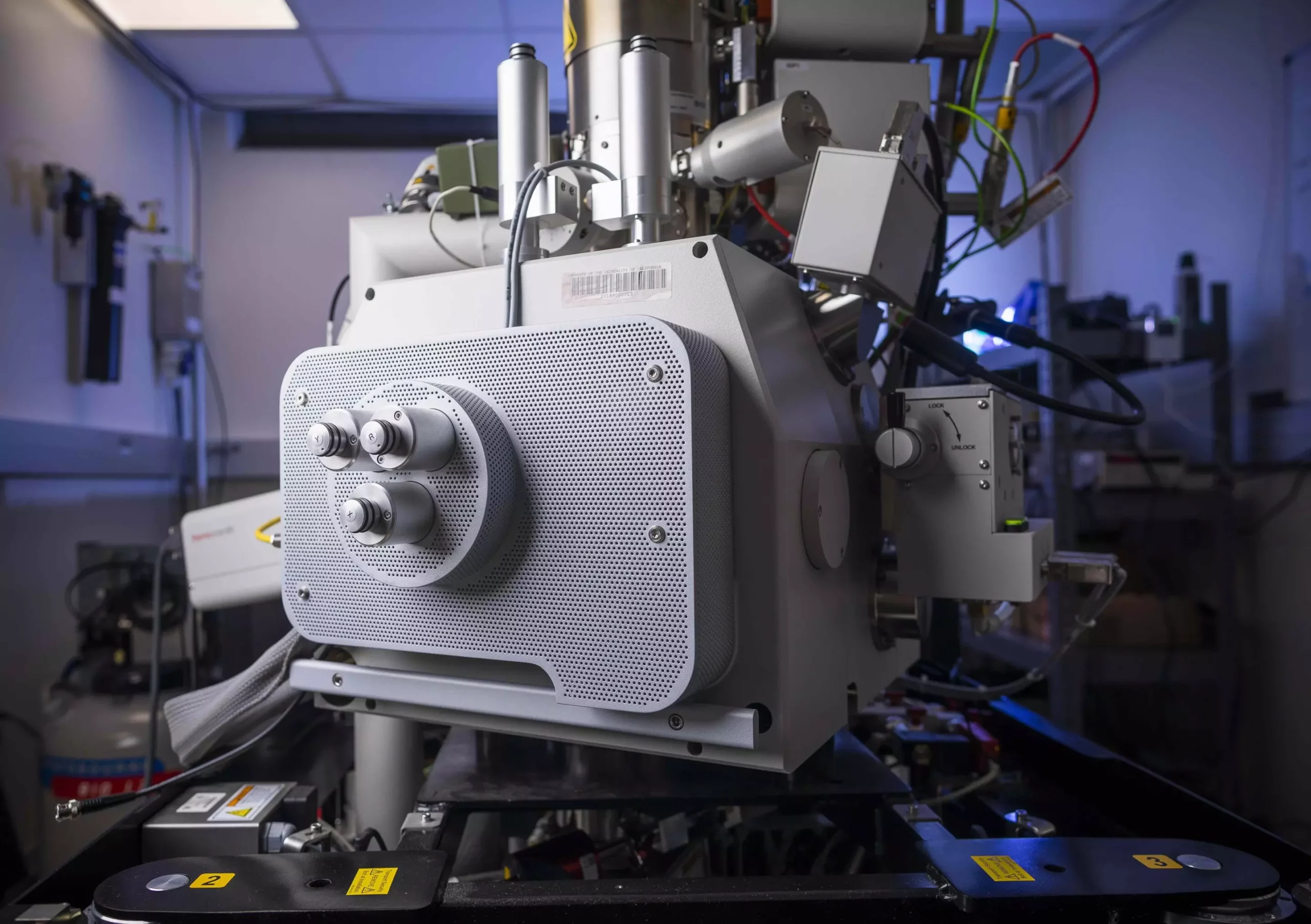
Advancements in semiconductor technology have taken a monumental leap forward with groundbreaking research from UC Santa Barbara. A research team, led by Associate Professor Bolin Liao, has pioneered a technique to create the first-ever “movie” capturing the movement of electric charges across the interface between two distinct semiconductor materials. This visualization, enabled by the application of scanning ultrafast electron microscopy (SUEM), sets the stage for a new era of direct observation in semiconductor research, challenging long-held theoretical assumptions and paving the way for future technological innovations.
Understanding the behavior of electric charges within semiconductors is crucial for improving the performance of devices such as solar cells, sensors, and lasers. Traditionally, the interaction between photocarriers—excited electrons and the accompanying “holes”—has been described primarily through theoretical frameworks and indirect measurements. As Liao pointed out, while textbooks abound with explanations, the ability to observe these phenomena in real-time has been lacking. The new imaging capabilities provide a much-needed tangible perspective on how charges interact and migrate at the junction between different materials—referred to as heterojunctions.
This research shines a light on a phenomenon that could lead to significant improvements in energy efficiency. Photocarriers, generated by light absorption in a semiconductor, typically lose most of their energy almost instantaneously, dissipating it as heat. As a result, only a small portion of their potential energy is harnessed for use in devices like solar panels and energy-generating technologies. By visualizing these hot carriers in their initial state, researchers can begin to strategize improvements aimed at capturing more energy before it converts to waste heat.
The innovative SUEM technique merges the principles of ultrafast laser technology and electron microscopy, allowing for unprecedented temporal resolution. The research team employed ultrafast laser pulses as a time-sensitive shutter, which synchronized with an electron beam scanning across the heterojunction of silicon and germanium. This synchronization enabled them to capture the rapid motion of photocarriers, creating a cinematic experience of electron movement at the microscopic level.
Key to this approach is the need to observe events happening over a picosecond to nanosecond timeframe. The results demonstrate that when charges are excited in uniform regions of silicon or germanium, they initially possess high speeds due to their elevated temperature. However, when excitation occurs closer to the junction of the two materials, charge carriers encounter a unique challenge—being trapped by the potential at the interface. This phenomenon results in reduced mobility, presenting a significant concern for device performance and efficiency.
The findings from this research not only confirm theoretical predictions regarding charge trapping but also unveil new avenues for improvement in semiconductor device design. With a better understanding of how charges behave at material interfaces, device engineers can tailor materials and junction designs to optimize charge mobility.
This research could have wide-reaching implications, particularly in the fields of photovoltaics and telecommunications, where silicon and germanium are commonly used. By directly observing the behavior of hot carriers at these junctions, the team at UC Santa Barbara could provide essential insights that transform how future devices are conceptualized and manufactured.
The significance of this research cannot be overstated, as it draws on a lineage of semiconductor innovation that dates back to the original ideas put forth by renowned engineer Herb Kroemer. Kroemer’s 1957 proposition that “the interface is the device” laid the groundwork for modern semiconductor technology. The ability now to visualize and analyze such interfaces embodies the realization of his vision, catalyzing a new chapter in semiconductor research.
As this technology evolves, the potential to develop even more efficient and advanced electronic devices becomes increasingly realistic. Overall, the work of Liao and his colleagues marks a critical milestone in the continued advancement of semiconductor science, allowing researchers and engineers to explore crucial questions about material behavior that were previously relegated to theoretical discussions.
The emergence of SUEM as a tool to visualize hot carriers at semiconductor interfaces represents a monumental shift in how we understand and innovate in the field of electronics, offering a promising horizon for energy-efficient technologies that could reshape our future.


Leave a Reply