Traditional electronics operate on a binary system, utilizing semiconductors to relay information in the form of “1s” and “0s.” This process hinges on the movement of charged carriers, notably electrons and holes, to facilitate data transmission. Although this foundational approach has underpinned modern technology for decades, it is fundamentally limited by its reliance on these carriers, which can only convey information through electric charge variation. Essentially, conventional methods are reaching a plateau where further amplification of performance and efficiency is constrained.
The Spintronics Revolution: A New Paradigm
Enter spintronics, a transformative approach that leverages an additional facet of electrons— their spin. The notion of spin transcends the traditional binary system, assigning binary values based on the orientation of an electron’s magnetic moment: an “up” spin represents a 1, while a “down” spin signifies a 0. This revolutionary method promises to enhance the data processing capacity dramatically, potentially ushering in a new era of electronics capable of handling significantly larger volumes of information. However, translating spintronics from theory to practice has long been a daunting hurdle, primarily because of the intricate requirements for manipulating and stabilizing electron spin orientations.
Challenges in Spin Orientation Manipulation
Despite decades of rigorous research, a major obstacle has persistently plagued the commercialization of spintronic devices: the difficulty in maintaining stable electron spin orientations. The conventional technique typically involves tuning spin orientation via ferromagnets and magnetic fields. However, this method is often encumbered by its complexity and unreliability. One of the critical issues identified is that carriers experience significant decay in their spin orientation when transitioning from high-conductivity materials, such as metallic ferromagnets, to lower conductivity substances like undoped silicon. This limitation has thwarted the widespread applications of spintronics in commercial devices.
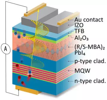
A Breakthrough Study: Transforming LEDs
Recent groundbreaking research, spearheaded by physicists at the University of Utah in collaboration with the National Renewable Energy Laboratory (NREL), has unveiled a novel approach to circumvent these limitations. The researchers modified off-the-shelf Light Emitting Diodes (LEDs), replacing one of the conventional electrodes with an innovative spin filter crafted from a hybrid organic-inorganic halide perovskite material. The remarkable result? The LEDs emitted circularly polarized light, a clear indication that the engineered design successfully enabled the injection of spin-aligned electrons into an existing semiconductor framework. This pivotal discovery may profoundly alter the trajectory of spintronics technologies, particularly in their integration with standard optoelectronic devices.
The Significance of Chiral Materials
At the crux of this innovation lies the introduction of chiral materials and their inherent properties. In previous studies, the research team examined chiral hybrid organic-inorganic halide perovskites, taking advantage of their unique symmetrical structures. The concept of chirality, reminiscent of the iconic left and right hands, entails that certain molecular configurations cannot be superimposed on their mirrored counterparts. By utilizing a “left-handed” oriented chiral layer, electrons with “up” spins can traverse the material, while “down” spins are obstructed. This remarkable property not only underscores the beauty of molecular design but also exemplifies the transformative potential of combining organic and inorganic materials in electronics.
The Innovation Process: A Simple Yet Profound Alteration
Implementing this technique was surprisingly straightforward. The team adeptly extracted one electrode from a conventional LED and substituted it with the spin filter, thereby enabling the ingress of spin-aligned electrons into the existing semiconductor architecture. The outcome was a remarkable display of highly circularly polarized light, signifying the operational success of this experimental device. The process involved stacking distinct layers within the LED, wherein each layer served a specific function: a transparent metallic electrode serves as a conductor, the chiral layer moderates electron spin direction, and the active layer generates light through electron recombination.
Future Implications of Spintronics
This research not only exemplifies the innovative potential of hybrid materials but also heralds an important shift for future technologies, including magnetic memory devices and advanced spintronic applications. The integration of spintronic principles could fundamentally redefine electronics, leading to devices with unprecedented efficiencies and capabilities. The leap from conventional electronic systems to spintronic interfaces poses intriguing possibilities: enhanced data storage, rapid processing speeds, and most importantly, a more sustainable and efficient electronic future.
As researchers continue to explore the underlying mechanisms and harness additional chiral materials—such as DNA—the stage is set for a transformative evolution in the field. The marvel of this discovery lies not just in its immediate applications but in the widening scope of future explorations in electronics. Now, as we stand on the cusp of a new technological revolution sparked by spintronics, it becomes evident that the future of electronics is not merely in progress but in a profound metamorphosis.
Leave a Reply